Stack Logo

980nm semiconductor laser becomes a powerful tool for plastic welding

Plastics are widely used in various industrial fields, and the demand for plastics in industrial production has gradually approached or even exceeded steel materials. Especially in the electronic manufacturing, medical, food packaging, automobile and other industries, plastic has become one of the indispensable key materials. The demand for precise and high-strength connection of various plastic parts in production is also increasing with the extensive use of plastic. And increasing day by day.

The choice of plastic parts connection technology has an important impact on the final application of plastic products. Traditional plastic connection processes include threaded connections, adhesive connections, insertion connections, press-fit connections, etc., as well as fusion connections represented by hot plate welding and ultrasonic welding. The advantages of these combination methods are simple operation, convenient connection, and strong applicability; but the disadvantages are also obvious, such as specific shape requirements and relatively low connection strength. When faced with complex irregular shapes such as three-dimensional geometric shapes, hollows, and large-scale Parts, and even plastic parts that have certain requirements for air tightness after connection, have small operating space and low efficiency.

Figure 2: Welding white structural parts.

At the same time, in the modern industrial field that pursues product innovation and quality improvement, the requirements for welding quality are getting higher and higher. With the development of laser technology, it has also promoted the gradual application of plastic welding technology. Laser plastic welding technology has become an important development direction and is gradually becoming the new favorite of connecting materials. It is often used for plastic parts of white household appliances, automobile plastic parts and other components. welding.

Laser plastic welding principle

Laser plastic welding, also known as laser translucent welding, requires that the upper plastic workpiece has high light transmittance and the lower workpiece can absorb laser energy. Therefore, the current mainstream welding objects are “transparent plastic + black plastic” and “transparent plastic + transparent plastic” combination method.

Since most transparent plastics have high light transmittance and low absorption in the 800nm~1100nm band, based on this, Nanofei Optoelectronics has launched a 980nm semiconductor laser, which integrates a high-precision control system in a compact structure and is easy to use. It uses advanced semiconductor laser technology to output near-infrared laser with a central wavelength of 980nm. The laser energy of this wavelength can penetrate the surface of transparent or translucent plastics, be absorbed by the lower layer and converted into heat energy, and can be used to implement precise and efficient plastic welding. The laser has high electro-optical conversion efficiency and provides continuous laser output. The power level can be selected according to the needs of the welding process. The output can be adjusted from several watts to hundreds of watts, making it suitable for large-area, high-speed plastic component welding operations. .

In addition to the laser body, the practical application of laser plastic welding also requires welding heads and welding fixtures. When using a 980nm semiconductor laser for plastic welding, first assemble the two parts to be welded together with the help of a fixture. The basic principle of welding is that the laser beam output by the welding head passes through the upper transparent plastic and is accurately projected to the lower plastic part under program control. The area to be welded; the lower plastic melts after absorbing the highly focused laser energy, and the contact surfaces of the upper and lower plastic parts are fully melted and combined through heat exchange. With the assistance of a certain external force, the weld is formed after cooling, and the final welding is completed. .

Welding circuit board plastic structural parts.

At the same time, with the help of a dedicated control system, precise heat control and local heating during the transmission welding process can be achieved, the welding quality is consistent, and adverse effects on surrounding materials are avoided. It is widely used in automotive parts, medical equipment, electronic components and other industries. Welding of precision plastic parts.

PC+ABS plastic welding test

In actual operation, in order to ensure weld quality and sufficient melting depth, it is necessary to comprehensively consider the relationship between welding speed and laser power to find the optimal process window.

Welding PC and ABS plastics were tested. The two plastic parts were first stacked on a carrier and clamped using a clamp to apply pressure.

When the laser output power is adjusted to 300W and the welding speed is set to 20mm/s (up to 10000mm/s), the two layers of plastic are welded successfully, the weld seam is evenly fused, the weld seam width is moderate, the sealing is good, and the tensile test strength reaches Require.

The laser output power remains unchanged at 300W. When the welding speed is reduced and adjusted to 10mm/s, the two layers of plastic are successfully welded, the welds are evenly fused, the welds are wide, and the sealing is good; however, due to the excessive temperature of the molten pool, it may cause Part of the material decomposes, resulting in reduced weld strength.

When the power is adjusted to 200W and the welding speed is set to 20mm/s, the weld width is moderate, the fusion is good, the sealing is good, and the tensile test strength is lower than the welding strength at high power.

Laser welding advantages

The processes of laser welding and fusion bonding are similar, but the advantages of the former are more obvious:

First of all, it has high precision. The laser spot is small and highly uniform. It can accurately align smaller welding parts, quickly convert laser energy into the energy required for welding, achieve precision welding, and greatly improve welding efficiency. . Combined with the professionally designed welding head, it can ensure that the laser energy is fully absorbed in the welding area and ensure the strength of the welding joint.

Secondly, the heat-affected zone is small, which can avoid thermal damage to the plastic surface during the welding process and maintain the transparency and smoothness of the material. This allows the product after light-transmitting welding to maintain its original appearance characteristics and enhance the structural stability.

Third, it solves the contradiction between welding speed and welding quality in traditional welding methods, can complete large-area welding in a short time, and greatly improves production efficiency. A welding job that originally took several hours can now be easily completed in just a few or dozens of minutes, saving a lot of time and cost.

In addition, the non-contact welding operation avoids the mechanical stress and vibration caused by traditional connection methods, protects the integrity of the plastic surface, and ensures the precision of the weld. The connection between materials is tighter and more reliable, and the sealing is excellent. , meeting high-standard product requirements such as waterproofing and dustproofing.

Figure 4: Welding automotive plastic parts

summary

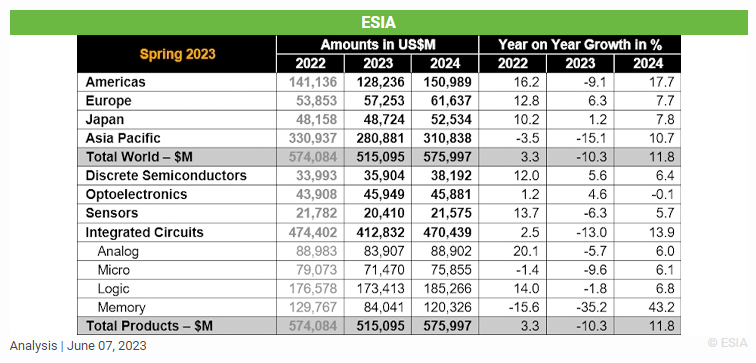
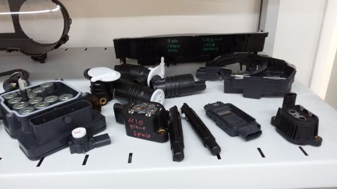
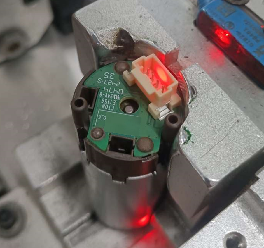
At present, the 980nm semiconductor laser has shown strong market potential and application value. It is a powerful tool for plastic welding, especially in automotive plastic welding, bringing efficient and stable welding results. In interior welding, it can be used for welding dashboards, center consoles, etc.; in exterior parts welding, it can easily weld door handles, lights, etc.; in welding automotive electronic parts, 980nm semiconductor lasers also perform well. , can be used for plastic welding of many electronic components, significantly improving the connection strength and sealing, ensuring the stability and reliability of each component. In the future, with the continuous development of functions, 980nm products will also usher in wider applications.

“Insanely Bullish For Humanity”: Hype Soars Around New “LK-99” Superconductor Material

There has been a lot of excitement on social media about the claim of a new superconductor that works at room temperature but also under ambient pressure. If the claims are true, the world could be nearing a new type of superconductor that some experts liken to the invention of the transistor. 

Last month, South Korean researchers published two new papers on what they say is a groundbreaking achievement: the development of a superconductor that operates at room temperature and standard atmospheric pressure. This is a huge step forward because, until now, all superconductors require low temperatures and high pressure to work, significantly restricting their real-world applications.

The superconductor utilizes a lead-based material has been called “LK-99.” Such a breakthrough would be a massive leap for more efficient energy transfer and the developing of more powerful maglev trains. 

Nick Cheng, an analyst at Jefferies Financial Group Inc., told clients, “If LK-99 is proved to be true and able to be mass-produced, it would be disruptive for a wide range of industries.” 

Cheng continued, “Cables could be made that transmit power without loss, saving energy, and advancements could be made in computer chips, rail transport and medical imaging as well.” 

“If true, the discovery would be one of the biggest ever in condensed matter physics and could usher in all sorts of technological marvels,” Science wrote.

China slaps export curbs on chipmaking metals in tech war warning to U.S., Europe

China is restricting the exports of two metals key to the manufacturing of semiconductors, its commerce ministry said late Monday, a warning to Europe and the United States in their escalating technological trade war over access to microchips.

These new regulations — imposed on grounds of national security — will require exporters to seek a license to ship some gallium and germanium compounds starting Aug. 1, China’s commerce ministry said. Applications for these export licenses must identify importers and end users and stipulate how these metals will be used.

This move is part of an intensifying global battle for technological supremacy — with China as the world’s largest source of both metals, according to a European Union study on critical raw materials this year. It also comes just as U.S. Treasury Secretary Janet Yellen is preparing to visit China later this week.

“This move will have a limited impact on global supply given the targeted scope,” Eurasia Group analysts, Anna Ashton, Xiaomeng Lu and Scott Young wrote in a note.

“It is a shot across the bow intended to remind countries including the United States, Japan, and the Netherlands that China has retaliatory options and to thereby deter them from imposing further restrictions on Chinese access to high-end chips and tools,” they added, pointing to the lack of outright bans for specific countries or end-users.

At a regular press conference in Beijing on Tuesday, China’s Ministry of Foreign Affairs spokesperson Mao Ning reiterated the country’s export controls are in accordance with the law and are not targeted at any specific country.

Shares of Chinese germanium producers soared on Tuesday in anticipation of rising prices for the raw materials, which may now face at least a short-term supply disruption.

On Tuesday, Yunnan Lincang Xinyuan Germanium Industrial surged by the 10% limit, closing at its highest in about 15 months in Shenzhen. Yunnan Chihong Zinc & Germanium ended up 6.1% at its highest level since mid-May in Shanghai. Both outperformed the 0.2% gain for the CSI 300 index of China’s largest A-share listings.

Limited short-term impact

South Korea’s industry ministry and Taiwan foreign ministry officials said Tuesday China’s curbs would have little short-term impact, Reuters reported.

Reuters further reported the South Korean industry ministry official as saying a possible expansion of curbs to include other materials cannot be ruled out.

Gallium is a soft silver metal used to produce compound semiconductor wafers for electronic circuits, semiconductors and light-emitting diodes, while germanium is used in the manufacturing of fiber optics to transfer data and information.

“The economies of scale in China’s extensive and increasingly integrated mining and processing operations, along with state subsidies, have allowed it to export processed minerals at a cost that operators elsewhere can’t match, perpetuating the country’s market dominance for many critical commodities,” Eurasia Group analysts said.

“But past Chinese attempts to leverage that dominance by restricting exports have reduced global availability and raised global prices. Higher prices have in turn spurred foreign competition by making mining and processing ventures outside of China more cost-competitive,” they added.

Festering feud

In October, the U.S. launched sweeping rules aimed at cutting off exports of key chips and semiconductor tools to China. The measures are believed to have the potential to cripple China’s ambitions to boost its domestic technology industries. The U.S. has also lobbied key chipmaking nations and allies, like the Netherlands and Japan, to introduce export restrictions of their own. The Netherlands responded Friday with new export restrictions on advanced semiconductor equipment. This will effectively bar ASML from exporting to China. But these latest Dutch curbs do not specifically target ASML, one of the most important semiconductor companies in the world.

Some countries are also trying to secure their own supply chains and build up their domestic chip industries, focusing on areas where they are traditionally strong. Last week, a fund backed by the Japanese government proposed a 903.9 billion yen ($6.3 billion) acquisition of semiconductor materials giant JSR.

Semiconductors are some of the most important technology products. They go into everything from smartphones to cars and refrigerators, and are also seen as key to military applications and advancing artificial intelligence.

Global semiconductor market expected to hit $515 billion in 2023

The global semiconductor market is predicted to reach USD 515 billion in 2023, or a downturn of 10.3%. However, this is anticipated to be followed by a robust recovery, with an estimated growth of 11.8% in 2024, reports the European Semiconductor Industry Association (ESIA).

The World Semiconductor Trade Statistics (WSTS) has adjusted its growth projections downwards in response to increasing inflation and weakening demand in end markets, particularly those relying on consumer spending. Although two primary categories, discrete and optoelectronics, are predicted to sustain single-digit year-over-year growth at 5.6% and 4.6% respectively in 2023, other categories are anticipated to shift into negative growth. This includes memory, which is forecasted to decline by approximately 35% year-over-year.

For 2023, the European and Japanese markets are projected to grow, with respective increases of 6.3% and 1.2%. Conversely, the remaining regions are anticipated to face a downturn, with the Americas expected to decline by 9.1% and the Asia Pacific region by 15.1%.

Global market is expected to rebound strongly in 2024

Looking ahead to 2024, the global semiconductor market is forecasted to surge by 11.8%, amounting to USD  576 billion. This expansion will primarily be driven by the memory segment, which is projected to recover to USD 120 billion in 2024, marking an increase of over 40% compared to the previous year. Nearly all other key categories, including discrete, sensors, analog, logic, and micro, are projected to exhibit single-digit growth.

In terms of regional perspectives, all areas are expected to see sustained growth in 2024. Notably, the Americas and Asia Pacific regions are estimated to showcase robust double-digit year-over-year growth.

The electronics components industry, as one of the most dynamic industries on the planet, regularly falls victim to its cyclicality – major swings from oversupply to severe allocations. The past two years have seen the market wrestle with a mix of transportation issues, large increases in demand, and at the same time severe shortages in many component families, some of which still exist today, during the current downturn.

Semiconductors: The Key to the Future of Electric Vehicles

It has often been said that cars these days are computers on wheels. Under the hood, there are hundreds of electronic control units (ECUs), essentially the brains controlling everything from the breaks and headlights to the latest gadgets such as parking cameras and radar. 

None of those comforts and conveniences would be possible without semiconductors – the tiny chips that make modern-day electronics tick. 

“Ninety percent of the innovations in the automobile industry actually come from the electronics and the chips are the soul of the electronics,” said Robert Li, vice president and general manager, PL driver and energy systems, NXP Semiconductors, one of the world’s largest chip manufacturers.

Li said next-generation chips could help solve some of the most pressing issues facing the EV industry, such as range and charge time, by making batteries more efficient. 

“Typically, if you buy a battery pack, a lot of times you can only use 80 to 90 percent of what is actually there because the measurement is not precise,” said Li. 

“The more high-performance, robust, safe and accurate electronics that you put in there, the more you can push that potential.” 

Even incremental gains in distance and charge time will matter in Europe, where EVs are seen as the linchpin to a green future. Plans are already under way to ban the sale of new combustion-engine cars by 2035, essentially eliminating one of the bloc’s biggest sources of CO2 emissions.

The more immediate challenge is a global chip shortage. EVs typically require hundreds, if not thousands, of more semiconductors than average combustion-engine cars and supplies could remain tight well into 2022. While production issues have already cropped up, most experts don’t expect any lasting effects when it comes to EV manufacturing and uptake. 

“Every manufacturer is having to pause production on certain models and they’re shuffling things around, trying to prioritize,” said Sam Abuelsamid, principal analyst e-,obility, Guidehouse Insights. “I think we’ll see less disruption to EVs because there is a need to get those vehicles out there, so they’re prioritizing EVs.” 

Abuelsamid said there was also a shift taking place within the auto industry to consolidate the hundreds of ECUs into just a handful of very powerful computers. 

“Down the road, we’re looking at even just one or two larger, more powerful computers. This should help resolve some of the problem,” he explained.

Cutting dependence on Asia

But with the vast majority of semiconductors manufactured in Asia, the chip shortage has served as a wake-up call for Europe. In her State of the European Union address in September, European Commission President Ursula von der Leyen specifically addressed the issue, saying that while demand for chips has risen, Europe’s share across the entire value chain has “shrunk.” 

“We depend right now on state-of-the-art chips manufactured by Asia. This is not just a matter of our competitiveness. This is also a matter of tech sovereignty. So let’s put all of our focus on it,” she said. 

Semiconductors will be key, not only to Europe’s green transition, but also it’s digital transformation, since they are the key component in everything from smartphones to smart cities.

Brussels is expected to present a new “Chips Act” in the coming weeks to bolster EU semiconductor capacity. But some experts have warned that trying to unravel a decades-old and deep supply chain may not have the desired results. 

“Manufacturing, especially cutting-edge manufacturing, will continue to be mainly provided in Taiwan and South Korea. If you take one of these out of the equation, the value chain kind of crumbles and you lose the ability to either develop or manufacture or package chips,” said Jan-Peter Kleinhans, project director for technology and geopolitics, Stiftung Neue Verantwortung.