The automobile wiring harness is the network main body of the automobile circuit. Without the wiring harness, there would be no automobile circuit. At present, whether it is a high-end luxury car or an economical ordinary car, whether it is a simple wiring harness or a complex wiring harness, the form is generally similar, and they are all composed of wires, connectors, protective sleeves and positioning parts.
They play the role of connection and power supply, ensuring the normal operation of the vehicle and the normal operation of various electronic devices. Automobile wiring harness has various functions. First of all, it plays the role of connecting electrical equipment. In the engine compartment of the car, various sensors, motors and electronic control modules need to be connected through wiring harnesses to achieve information transmission and interaction.
Secondly, the wiring harness is also responsible for transmitting power signals and providing power support for various systems, such as ignition systems, lighting systems, air conditioning systems, etc. Most importantly, the wiring harness can also prevent damage to the wires caused by friction, vibration or moisture, improving the stability and safety of the vehicle.
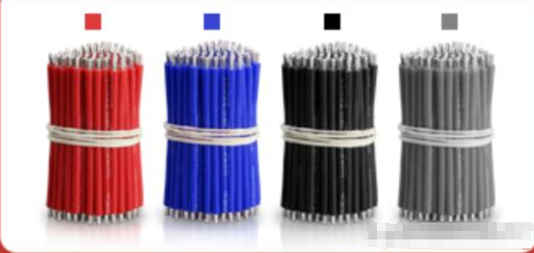
Thread colors in automotive wiring harnesses
Wire color: In order to facilitate the maintenance of automobile electrical systems, low-voltage wires are usually distinguished by different colors. The color of the wire insulation layer used today is generally two-color, consisting of a primary color and a secondary color. The main color is the base color of the wire, and the secondary color is the axial stripe color stripe on the wire. Commonly used colors are red, yellow, blue, green, black, white, brown, purple, gray, etc.
The buzz around pursuing smaller, more efficient transistors has led to a deep interest in using 2D TMDs instead of Si Gate all-around (GAA) nanoribbons (NRs) below the 10nm gate length. At this tiny scale, Si faces issues like direct tunneling causing leakage, while 2D TMDs step in with their solid band gap and sustained mobilities, offering solutions to these hurdles. In the GAA NR structures, 2D TMDs showcase a scaling advantage: you can fit six 2D TMD NRs for every four Si NRs, potentially hinting at superior performance in the same space. These inherent physical benefits promise significant scaling potential.
Fabricating 2D TMD GAA NRs requires key steps like deposition, etching to form channels, doping, and contact/gate formation. However, each stage faces obstacles compared to established Si approaches. Etching TMD layers into nano-channels risks edge defects affecting performance and relies on selective chemistries that avoid harming delicate monolayers. Forming quality contacts requires optimizing exposed TMD surface area while minimizing material degradation from etching, unlike Si, conventional ion implantation doping methods damage TMDs, necessitating remote charge-based approaches that introduce coulombic scattering. Depositing effective gate oxides also struggle for a lack of dangling bonds to initiate controlled growth. Additionally, the overall mechanical fragility of atomically thin TMDs makes them vulnerable to internal stresses during processing.
Realizing the promise of 2D TMDs necessitates advancing their growth quality closer to the epitaxial precision of Si GAA NRs. Silicon’s unmatched defect densities have enabled its perseverance as the material of choice for over 50 years. Lateral growth from random nucleation sites results in polycrystalline morphologies with performance-sapping grain boundaries. Compounding this issue is the conflict between existing approaches to tackle contact resistance, primarily based on evaporated top contacts and the implicit preference for edge contacts in the simplest fabrication of NR transistors. A potential solution involves altering etch sequences to form a partial wrap-around contact, albeit potentially impacting transistor density.
Advancements in 2D TMD growth, contact resistance mitigation, and innovative fabrication techniques will likely pave the way for these materials to revolutionize the semiconductor industry, potentially rivaling or outperforming the capabilities of Si-based technology.
Plastics are widely used in various industrial fields, and the demand for plastics in industrial production has gradually approached or even exceeded steel materials. Especially in the electronic manufacturing, medical, food packaging, automobile and other industries, plastic has become one of the indispensable key materials. The demand for precise and high-strength connection of various plastic parts in production is also increasing with the extensive use of plastic. And increasing day by day.
The choice of plastic parts connection technology has an important impact on the final application of plastic products. Traditional plastic connection processes include threaded connections, adhesive connections, insertion connections, press-fit connections, etc., as well as fusion connections represented by hot plate welding and ultrasonic welding. The advantages of these combination methods are simple operation, convenient connection, and strong applicability; but the disadvantages are also obvious, such as specific shape requirements and relatively low connection strength. When faced with complex irregular shapes such as three-dimensional geometric shapes, hollows, and large-scale Parts, and even plastic parts that have certain requirements for air tightness after connection, have small operating space and low efficiency.
Figure 2: Welding white structural parts.
At the same time, in the modern industrial field that pursues product innovation and quality improvement, the requirements for welding quality are getting higher and higher. With the development of laser technology, it has also promoted the gradual application of plastic welding technology. Laser plastic welding technology has become an important development direction and is gradually becoming the new favorite of connecting materials. It is often used for plastic parts of white household appliances, automobile plastic parts and other components. welding.
Laser plastic welding principle
Laser plastic welding, also known as laser translucent welding, requires that the upper plastic workpiece has high light transmittance and the lower workpiece can absorb laser energy. Therefore, the current mainstream welding objects are “transparent plastic + black plastic” and “transparent plastic + transparent plastic” combination method.
Since most transparent plastics have high light transmittance and low absorption in the 800nm~1100nm band, based on this, Nanofei Optoelectronics has launched a 980nm semiconductor laser, which integrates a high-precision control system in a compact structure and is easy to use. It uses advanced semiconductor laser technology to output near-infrared laser with a central wavelength of 980nm. The laser energy of this wavelength can penetrate the surface of transparent or translucent plastics, be absorbed by the lower layer and converted into heat energy, and can be used to implement precise and efficient plastic welding. The laser has high electro-optical conversion efficiency and provides continuous laser output. The power level can be selected according to the needs of the welding process. The output can be adjusted from several watts to hundreds of watts, making it suitable for large-area, high-speed plastic component welding operations. .
In addition to the laser body, the practical application of laser plastic welding also requires welding heads and welding fixtures. When using a 980nm semiconductor laser for plastic welding, first assemble the two parts to be welded together with the help of a fixture. The basic principle of welding is that the laser beam output by the welding head passes through the upper transparent plastic and is accurately projected to the lower plastic part under program control. The area to be welded; the lower plastic melts after absorbing the highly focused laser energy, and the contact surfaces of the upper and lower plastic parts are fully melted and combined through heat exchange. With the assistance of a certain external force, the weld is formed after cooling, and the final welding is completed. .
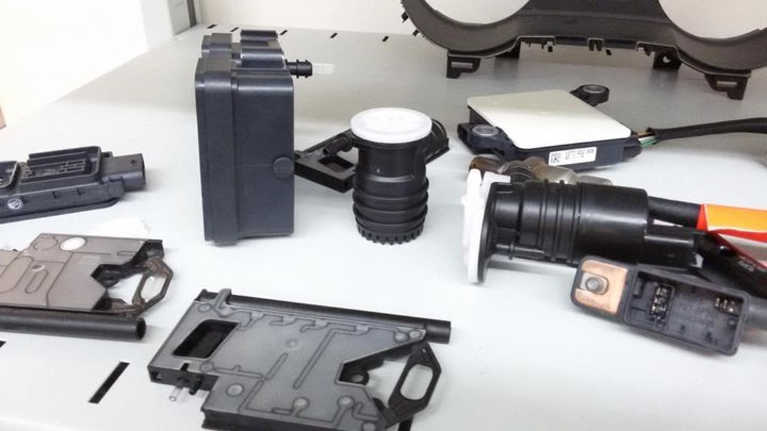
Welding circuit board plastic structural parts.
At the same time, with the help of a dedicated control system, precise heat control and local heating during the transmission welding process can be achieved, the welding quality is consistent, and adverse effects on surrounding materials are avoided. It is widely used in automotive parts, medical equipment, electronic components and other industries. Welding of precision plastic parts.
PC+ABS plastic welding test
In actual operation, in order to ensure weld quality and sufficient melting depth, it is necessary to comprehensively consider the relationship between welding speed and laser power to find the optimal process window.
Welding PC and ABS plastics were tested. The two plastic parts were first stacked on a carrier and clamped using a clamp to apply pressure.
When the laser output power is adjusted to 300W and the welding speed is set to 20mm/s (up to 10000mm/s), the two layers of plastic are welded successfully, the weld seam is evenly fused, the weld seam width is moderate, the sealing is good, and the tensile test strength reaches Require.
The laser output power remains unchanged at 300W. When the welding speed is reduced and adjusted to 10mm/s, the two layers of plastic are successfully welded, the welds are evenly fused, the welds are wide, and the sealing is good; however, due to the excessive temperature of the molten pool, it may cause Part of the material decomposes, resulting in reduced weld strength.
When the power is adjusted to 200W and the welding speed is set to 20mm/s, the weld width is moderate, the fusion is good, the sealing is good, and the tensile test strength is lower than the welding strength at high power.
Laser welding advantages
The processes of laser welding and fusion bonding are similar, but the advantages of the former are more obvious:
First of all, it has high precision. The laser spot is small and highly uniform. It can accurately align smaller welding parts, quickly convert laser energy into the energy required for welding, achieve precision welding, and greatly improve welding efficiency. . Combined with the professionally designed welding head, it can ensure that the laser energy is fully absorbed in the welding area and ensure the strength of the welding joint.
Secondly, the heat-affected zone is small, which can avoid thermal damage to the plastic surface during the welding process and maintain the transparency and smoothness of the material. This allows the product after light-transmitting welding to maintain its original appearance characteristics and enhance the structural stability.
Third, it solves the contradiction between welding speed and welding quality in traditional welding methods, can complete large-area welding in a short time, and greatly improves production efficiency. A welding job that originally took several hours can now be easily completed in just a few or dozens of minutes, saving a lot of time and cost.
In addition, the non-contact welding operation avoids the mechanical stress and vibration caused by traditional connection methods, protects the integrity of the plastic surface, and ensures the precision of the weld. The connection between materials is tighter and more reliable, and the sealing is excellent. , meeting high-standard product requirements such as waterproofing and dustproofing.
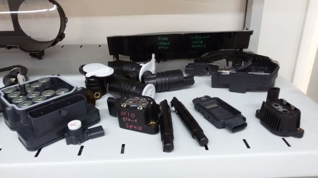
Figure 4: Welding automotive plastic parts
summary
At present, the 980nm semiconductor laser has shown strong market potential and application value. It is a powerful tool for plastic welding, especially in automotive plastic welding, bringing efficient and stable welding results. In interior welding, it can be used for welding dashboards, center consoles, etc.; in exterior parts welding, it can easily weld door handles, lights, etc.; in welding automotive electronic parts, 980nm semiconductor lasers also perform well. , can be used for plastic welding of many electronic components, significantly improving the connection strength and sealing, ensuring the stability and reliability of each component. In the future, with the continuous development of functions, 980nm products will also usher in wider applications.
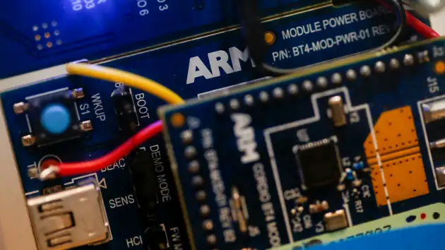
The news indicates that Apple has secured access to a core piece of intellectual property, the Arm architecture, used in its iPhone and Mac chips, for the foreseeable future.
Arm, owned by SoftBank, is set to debut on the Nasdaq stock exchange in the coming weeks at a total valuation that could be as high as $52 billion, which would be the biggest technology initial public offering this year.
For Arm, its note about the Apple deal indicates that at least one of its most important partners will continue to use the company’s technology for years, quelling some fears that the change in Arm’s corporate structure could prompt some of its customers into looking for technological alternatives.
“Further, we have entered into a new long-term agreement with Apple that extends beyond 2040, continuing our longstanding relationship of collaboration with Apple and Apple’s access to the Arm architecture,” Arm said in its updated SEC filing.
Arm’s architecture is used in nearly every smartphone chip, including Apple’s A-series for iPhones. Arm’s instruction set outlines how a central processor works at its most basic level, such as how to do arithmetic or access computer memory. Switching large software projects to other instruction sets is expensive, difficult and time consuming.
Arm, originally founded in 1990, started growing fiercely after the iPhone came out in 2007 and smartphone makers needed chips that were geared for low-power usage, especially compared with the x86 architecture used in PC and server chips by Intel and AMD.
Cornerstone investors
One reason firms such as Apple use Arm’s architecture is because it has not been owned by a competitor. Arm, a British company, licensed its technology to all comers, and its customers could plan to invest billions in developing Arm chips without worrying that their access to the technology could be curtailed.
The company said 250 billion chips have shipped using Arm’s architecture, although about half the company’s royalties revenue comes from products released between 1990 and 2012, according to the filing.
Concerns over access to Arm technology is one of the main reasons regulators blocked Nvidia’s bid to buy Arm early last year, leading to this fall’s IPO.
Apple, Google, Nvidia, Samsung, AMD, Intel, Cadence, Synopsis, Samsung and Taiwan Semiconductor Manufacturing Company have expressed interest in buying some Arm shares as part of the offering, as much as $735 million in total according to the filing, which would give those companies a stake in Arm’s ownership and some say in how it is managed. They’re referred to as “cornerstone investors.”
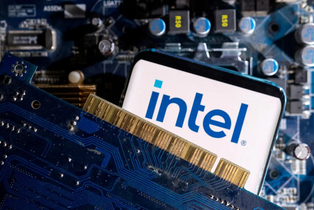
Intel calls off its planned acquisition of Tower Semiconductor, an Israeli chip maker, after waiting in vain for 18 months for a review by Chinese regulators.
China has effectively scuttled a $5.4 billion deal by Intel, the Silicon Valley semiconductor giant, in the latest sign of the frayed business ties between China and the United States.
Intel, which has long had operations in China, said Wednesday that it had “mutually agreed” to terminate a planned merger with Tower Semiconductor, an Israeli chip manufacturer. The announcement came after China’s antitrust regulators failed to rule on the transaction before a deadline set by the companies.
The failure of Intel to complete the acquisition of Tower could send a further chill through American companies with deep ties in China, where it is becoming increasingly difficult to do business amid tensions between the two countries.
The planned merger, announced in February 2022, passed an antitrust review in the United States and several other geographies. But it ran into a lengthy delay in China, where regulators review mergers of companies that earn a certain amount of revenue in the country.
Technology is the prime battlefield in the tense economic relations between China and the United States.
Beijing is deeply upset by an American-led set of international restrictions on the sale to China of the most advanced computer chips, which have military applications, and of the factory equipment to make such chips. Those restrictions were put in place in October. In a separate action, President Biden last week ordered a ban on certain new investments in sensitive Chinese technology.
China has condemned the moves as an effort by Washington to throttle its tech development and slow its economic growth.
Despite the raw tensions between the countries, their economies remain highly interconnected, dependent on one another’s supply chains, technology and investment money.
For Intel, China is both a major marketplace and place of business: In 2022, the company employed more than 12,000 people there, and made more than $17 billion in revenue, about 27 percent of its global total. It started doing business in China in the mid-1980s, with operations that include assembling and testing chips manufactured elsewhere.
Intel, which is struggling to regain a lead in chip production technology, hoped the merger with Tower would help accelerate a shift to become a major manufacturer for other designers of chips. Intel has previously mainly used its factories to produce chips it both designs and sells.
Tower, which has an office in Shanghai, was founded in 1993 and operates a relatively small chip manufacturing service compared with giants like Taiwan Semiconductor Manufacturing Company. Intel will pay Tower $353 million for failing to close the deal, according to a statement by Intel.
Intel’s inability to get the merger approved in China underlines what could become an increasingly hard choice for multinationals: They may need to choose between having operations in China or carrying out mergers and acquisitions around the globe. Such concerns could produce a further chill on foreign investment in China, which has already plunged this year because of geopolitical concerns.
The Chinese government agency that decides whether to approve global mergers, the State Administration for Market Regulation, is now “in an uncomfortable spotlight as a proxy for China’s commitment to market access for foreign investors,” said Han Shen Lin, the China country director for The Asia Group, an advisory firm in Washington.
Before the agency was established in 2018, global mergers were reviewed in China mainly by a unit of the Ministry of Commerce, which is dominated by civil servants with extensive international experience and contact with foreign businesses and governments.
The State Administration for Market Regulation, by contrast, is categorized within the Chinese bureaucracy as primarily a domestic agency, and its officials have shunned most contact with foreign governments, embassies or businesses.
Patrick Gelsinger, who became Intel’s chief executive in early 2021, has pushed to add what the industry calls chip foundry services, in part to attract U.S. government subsidies under legislation passed a year ago. He recently traveled to China to help get the Tower deal approved.
“We continue to drive forward on all facets of our strategy,” Mr. Gelsinger said in a statement on Wednesday.
Intel’s fabrication plants, or fabs, tend to specialize in advanced production processes used to make microprocessors and other digital chips. Tower, by contrast, is best-known for older technology that produces analog chips, which are used for jobs like amplifying signals and managing power in cellphones and other products.
The company now owns two fabs in Israel, two in the United States, three in Japan and is participating in a joint manufacturing venture in Italy.
There has been a lot of excitement on social media about the claim of a new superconductor that works at room temperature but also under ambient pressure. If the claims are true, the world could be nearing a new type of superconductor that some experts liken to the invention of the transistor.
Last month, South Korean researchers published two new papers on what they say is a groundbreaking achievement: the development of a superconductor that operates at room temperature and standard atmospheric pressure. This is a huge step forward because, until now, all superconductors require low temperatures and high pressure to work, significantly restricting their real-world applications.
The superconductor utilizes a lead-based material has been called “LK-99.” Such a breakthrough would be a massive leap for more efficient energy transfer and the developing of more powerful maglev trains.
Nick Cheng, an analyst at Jefferies Financial Group Inc., told clients, “If LK-99 is proved to be true and able to be mass-produced, it would be disruptive for a wide range of industries.”
Cheng continued, “Cables could be made that transmit power without loss, saving energy, and advancements could be made in computer chips, rail transport and medical imaging as well.”
“If true, the discovery would be one of the biggest ever in condensed matter physics and could usher in all sorts of technological marvels,” Science wrote.
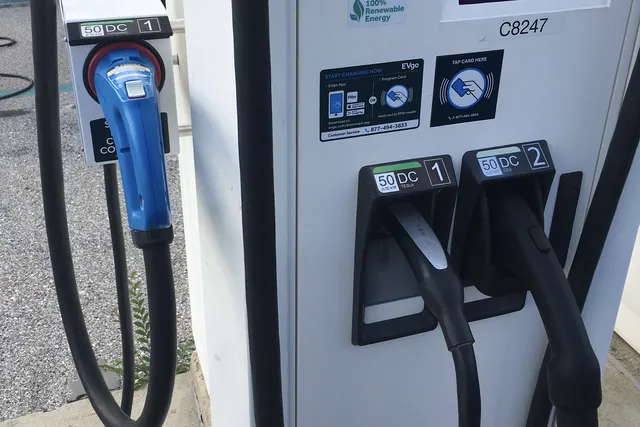
BMW, GM, Honda, Hyundai, Kia, Mercedes-Benz, and Stellantis are creating a joint venture to launch a public charging network in North America.
A new group of automotive super friends is banding together, promising to build the next big North American electric vehicle charging network. These worldwide automakers — BMW, General Motors, Honda, Hyundai, Kia, Mercedes-Benz, and Stellantis — announced a planned joint venture today to erect easy-to-activate DC fast chargers along US and Canadian highways and in urban environments.
The grand plan for the currently unnamed partnership is to install “at least” 30,000 high-speed EV chargers by 2030, with the first ones to open summer 2024 in the US. The collective plans to leverage National Electric Vehicle Infrastructure (NEVI) funding in the US and will also use other private and public funding from state and federal sources to build out the network.
Current EV charging networks, from Tesla Superchargers to Electrify America, have stations installed in places where people can shop, eat, and use the bathroom. In a similar fashion, these new chargers will also be installed along routes to vacation destinations and in metropolitan areas.
The new stations will connect and charge EV models made by the partnered automakers without having to fumble with another charging station app. The companies also plan to integrate the developing “Plug and Charge” standard that the Federal Highway Administration is attempting to standardize.
“The better experience people have, the faster EV adoption will grow,” GM CEO Mary Barra states in the joint venture press release. Many charging networks today require their own apps and have issues of reliability. Tesla’s Supercharger network, which is considered among the best in the world, will be available to vehicles from automakers including Ford, GM, Volvo, and more without needing people to activate with an app.
The new joint venture is also planned to be entirely powered by renewable energy. It’s not known if renewable energy will directly power them or if the companies plan to buy credits like Rivian announced yesterday.
China is restricting the exports of two metals key to the manufacturing of semiconductors, its commerce ministry said late Monday, a warning to Europe and the United States in their escalating technological trade war over access to microchips.
These new regulations — imposed on grounds of national security — will require exporters to seek a license to ship some gallium and germanium compounds starting Aug. 1, China’s commerce ministry said. Applications for these export licenses must identify importers and end users and stipulate how these metals will be used.
This move is part of an intensifying global battle for technological supremacy — with China as the world’s largest source of both metals, according to a European Union study on critical raw materials this year. It also comes just as U.S. Treasury Secretary Janet Yellen is preparing to visit China later this week.
“This move will have a limited impact on global supply given the targeted scope,” Eurasia Group analysts, Anna Ashton, Xiaomeng Lu and Scott Young wrote in a note.
“It is a shot across the bow intended to remind countries including the United States, Japan, and the Netherlands that China has retaliatory options and to thereby deter them from imposing further restrictions on Chinese access to high-end chips and tools,” they added, pointing to the lack of outright bans for specific countries or end-users.
At a regular press conference in Beijing on Tuesday, China’s Ministry of Foreign Affairs spokesperson Mao Ning reiterated the country’s export controls are in accordance with the law and are not targeted at any specific country.
Shares of Chinese germanium producers soared on Tuesday in anticipation of rising prices for the raw materials, which may now face at least a short-term supply disruption.
On Tuesday, Yunnan Lincang Xinyuan Germanium Industrial surged by the 10% limit, closing at its highest in about 15 months in Shenzhen. Yunnan Chihong Zinc & Germanium ended up 6.1% at its highest level since mid-May in Shanghai. Both outperformed the 0.2% gain for the CSI 300 index of China’s largest A-share listings.
Limited short-term impact
South Korea’s industry ministry and Taiwan foreign ministry officials said Tuesday China’s curbs would have little short-term impact, Reuters reported.
Reuters further reported the South Korean industry ministry official as saying a possible expansion of curbs to include other materials cannot be ruled out.
Gallium is a soft silver metal used to produce compound semiconductor wafers for electronic circuits, semiconductors and light-emitting diodes, while germanium is used in the manufacturing of fiber optics to transfer data and information.
“The economies of scale in China’s extensive and increasingly integrated mining and processing operations, along with state subsidies, have allowed it to export processed minerals at a cost that operators elsewhere can’t match, perpetuating the country’s market dominance for many critical commodities,” Eurasia Group analysts said.
“But past Chinese attempts to leverage that dominance by restricting exports have reduced global availability and raised global prices. Higher prices have in turn spurred foreign competition by making mining and processing ventures outside of China more cost-competitive,” they added.
Some countries are also trying to secure their own supply chains and build up their domestic chip industries, focusing on areas where they are traditionally strong. Last week, a fund backed by the Japanese government proposed a 903.9 billion yen ($6.3 billion) acquisition of semiconductor materials giant JSR.
Semiconductors are some of the most important technology products. They go into everything from smartphones to cars and refrigerators, and are also seen as key to military applications and advancing artificial intelligence.
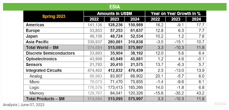
The global semiconductor market is predicted to reach USD 515 billion in 2023, or a downturn of 10.3%. However, this is anticipated to be followed by a robust recovery, with an estimated growth of 11.8% in 2024, reports the European Semiconductor Industry Association (ESIA).
The World Semiconductor Trade Statistics (WSTS) has adjusted its growth projections downwards in response to increasing inflation and weakening demand in end markets, particularly those relying on consumer spending. Although two primary categories, discrete and optoelectronics, are predicted to sustain single-digit year-over-year growth at 5.6% and 4.6% respectively in 2023, other categories are anticipated to shift into negative growth. This includes memory, which is forecasted to decline by approximately 35% year-over-year.
For 2023, the European and Japanese markets are projected to grow, with respective increases of 6.3% and 1.2%. Conversely, the remaining regions are anticipated to face a downturn, with the Americas expected to decline by 9.1% and the Asia Pacific region by 15.1%.
Global market is expected to rebound strongly in 2024
Looking ahead to 2024, the global semiconductor market is forecasted to surge by 11.8%, amounting to USD 576 billion. This expansion will primarily be driven by the memory segment, which is projected to recover to USD 120 billion in 2024, marking an increase of over 40% compared to the previous year. Nearly all other key categories, including discrete, sensors, analog, logic, and micro, are projected to exhibit single-digit growth.
In terms of regional perspectives, all areas are expected to see sustained growth in 2024. Notably, the Americas and Asia Pacific regions are estimated to showcase robust double-digit year-over-year growth.
The electronics components industry, as one of the most dynamic industries on the planet, regularly falls victim to its cyclicality – major swings from oversupply to severe allocations. The past two years have seen the market wrestle with a mix of transportation issues, large increases in demand, and at the same time severe shortages in many component families, some of which still exist today, during the current downturn.