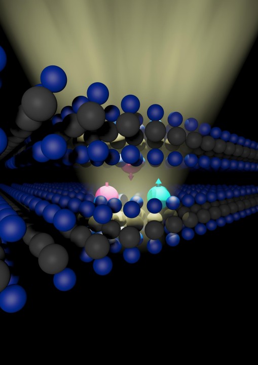
The buzz around pursuing smaller, more efficient transistors has led to a deep interest in using 2D TMDs instead of Si Gate all-around (GAA) nanoribbons (NRs) below the 10nm gate length. At this tiny scale, Si faces issues like direct tunneling causing leakage, while 2D TMDs step in with their solid band gap and sustained mobilities, offering solutions to these hurdles. In the GAA NR structures, 2D TMDs showcase a scaling advantage: you can fit six 2D TMD NRs for every four Si NRs, potentially hinting at superior performance in the same space. These inherent physical benefits promise significant scaling potential.
Fabricating 2D TMD GAA NRs requires key steps like deposition, etching to form channels, doping, and contact/gate formation. However, each stage faces obstacles compared to established Si approaches. Etching TMD layers into nano-channels risks edge defects affecting performance and relies on selective chemistries that avoid harming delicate monolayers. Forming quality contacts requires optimizing exposed TMD surface area while minimizing material degradation from etching, unlike Si, conventional ion implantation doping methods damage TMDs, necessitating remote charge-based approaches that introduce coulombic scattering. Depositing effective gate oxides also struggle for a lack of dangling bonds to initiate controlled growth. Additionally, the overall mechanical fragility of atomically thin TMDs makes them vulnerable to internal stresses during processing.
Realizing the promise of 2D TMDs necessitates advancing their growth quality closer to the epitaxial precision of Si GAA NRs. Silicon’s unmatched defect densities have enabled its perseverance as the material of choice for over 50 years. Lateral growth from random nucleation sites results in polycrystalline morphologies with performance-sapping grain boundaries. Compounding this issue is the conflict between existing approaches to tackle contact resistance, primarily based on evaporated top contacts and the implicit preference for edge contacts in the simplest fabrication of NR transistors. A potential solution involves altering etch sequences to form a partial wrap-around contact, albeit potentially impacting transistor density.
Advancements in 2D TMD growth, contact resistance mitigation, and innovative fabrication techniques will likely pave the way for these materials to revolutionize the semiconductor industry, potentially rivaling or outperforming the capabilities of Si-based technology.

