The automobile wiring harness is the network main body of the automobile circuit. Without the wiring harness, there would be no automobile circuit. At present, whether it is a high-end luxury car or an economical ordinary car, whether it is a simple wiring harness or a complex wiring harness, the form is generally similar, and they are all composed of wires, connectors, protective sleeves and positioning parts.
They play the role of connection and power supply, ensuring the normal operation of the vehicle and the normal operation of various electronic devices. Automobile wiring harness has various functions. First of all, it plays the role of connecting electrical equipment. In the engine compartment of the car, various sensors, motors and electronic control modules need to be connected through wiring harnesses to achieve information transmission and interaction.
Secondly, the wiring harness is also responsible for transmitting power signals and providing power support for various systems, such as ignition systems, lighting systems, air conditioning systems, etc. Most importantly, the wiring harness can also prevent damage to the wires caused by friction, vibration or moisture, improving the stability and safety of the vehicle.
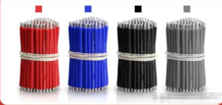
Thread colors in automotive wiring harnesses
Wire color: In order to facilitate the maintenance of automobile electrical systems, low-voltage wires are usually distinguished by different colors. The color of the wire insulation layer used today is generally two-color, consisting of a primary color and a secondary color. The main color is the base color of the wire, and the secondary color is the axial stripe color stripe on the wire. Commonly used colors are red, yellow, blue, green, black, white, brown, purple, gray, etc.
The buzz around pursuing smaller, more efficient transistors has led to a deep interest in using 2D TMDs instead of Si Gate all-around (GAA) nanoribbons (NRs) below the 10nm gate length. At this tiny scale, Si faces issues like direct tunneling causing leakage, while 2D TMDs step in with their solid band gap and sustained mobilities, offering solutions to these hurdles. In the GAA NR structures, 2D TMDs showcase a scaling advantage: you can fit six 2D TMD NRs for every four Si NRs, potentially hinting at superior performance in the same space. These inherent physical benefits promise significant scaling potential.
Fabricating 2D TMD GAA NRs requires key steps like deposition, etching to form channels, doping, and contact/gate formation. However, each stage faces obstacles compared to established Si approaches. Etching TMD layers into nano-channels risks edge defects affecting performance and relies on selective chemistries that avoid harming delicate monolayers. Forming quality contacts requires optimizing exposed TMD surface area while minimizing material degradation from etching, unlike Si, conventional ion implantation doping methods damage TMDs, necessitating remote charge-based approaches that introduce coulombic scattering. Depositing effective gate oxides also struggle for a lack of dangling bonds to initiate controlled growth. Additionally, the overall mechanical fragility of atomically thin TMDs makes them vulnerable to internal stresses during processing.
Realizing the promise of 2D TMDs necessitates advancing their growth quality closer to the epitaxial precision of Si GAA NRs. Silicon’s unmatched defect densities have enabled its perseverance as the material of choice for over 50 years. Lateral growth from random nucleation sites results in polycrystalline morphologies with performance-sapping grain boundaries. Compounding this issue is the conflict between existing approaches to tackle contact resistance, primarily based on evaporated top contacts and the implicit preference for edge contacts in the simplest fabrication of NR transistors. A potential solution involves altering etch sequences to form a partial wrap-around contact, albeit potentially impacting transistor density.
Advancements in 2D TMD growth, contact resistance mitigation, and innovative fabrication techniques will likely pave the way for these materials to revolutionize the semiconductor industry, potentially rivaling or outperforming the capabilities of Si-based technology.
Plastics are widely used in various industrial fields, and the demand for plastics in industrial production has gradually approached or even exceeded steel materials. Especially in the electronic manufacturing, medical, food packaging, automobile and other industries, plastic has become one of the indispensable key materials. The demand for precise and high-strength connection of various plastic parts in production is also increasing with the extensive use of plastic. And increasing day by day.
The choice of plastic parts connection technology has an important impact on the final application of plastic products. Traditional plastic connection processes include threaded connections, adhesive connections, insertion connections, press-fit connections, etc., as well as fusion connections represented by hot plate welding and ultrasonic welding. The advantages of these combination methods are simple operation, convenient connection, and strong applicability; but the disadvantages are also obvious, such as specific shape requirements and relatively low connection strength. When faced with complex irregular shapes such as three-dimensional geometric shapes, hollows, and large-scale Parts, and even plastic parts that have certain requirements for air tightness after connection, have small operating space and low efficiency.
Figure 2: Welding white structural parts.
At the same time, in the modern industrial field that pursues product innovation and quality improvement, the requirements for welding quality are getting higher and higher. With the development of laser technology, it has also promoted the gradual application of plastic welding technology. Laser plastic welding technology has become an important development direction and is gradually becoming the new favorite of connecting materials. It is often used for plastic parts of white household appliances, automobile plastic parts and other components. welding.
Laser plastic welding principle
Laser plastic welding, also known as laser translucent welding, requires that the upper plastic workpiece has high light transmittance and the lower workpiece can absorb laser energy. Therefore, the current mainstream welding objects are “transparent plastic + black plastic” and “transparent plastic + transparent plastic” combination method.
Since most transparent plastics have high light transmittance and low absorption in the 800nm~1100nm band, based on this, Nanofei Optoelectronics has launched a 980nm semiconductor laser, which integrates a high-precision control system in a compact structure and is easy to use. It uses advanced semiconductor laser technology to output near-infrared laser with a central wavelength of 980nm. The laser energy of this wavelength can penetrate the surface of transparent or translucent plastics, be absorbed by the lower layer and converted into heat energy, and can be used to implement precise and efficient plastic welding. The laser has high electro-optical conversion efficiency and provides continuous laser output. The power level can be selected according to the needs of the welding process. The output can be adjusted from several watts to hundreds of watts, making it suitable for large-area, high-speed plastic component welding operations. .
In addition to the laser body, the practical application of laser plastic welding also requires welding heads and welding fixtures. When using a 980nm semiconductor laser for plastic welding, first assemble the two parts to be welded together with the help of a fixture. The basic principle of welding is that the laser beam output by the welding head passes through the upper transparent plastic and is accurately projected to the lower plastic part under program control. The area to be welded; the lower plastic melts after absorbing the highly focused laser energy, and the contact surfaces of the upper and lower plastic parts are fully melted and combined through heat exchange. With the assistance of a certain external force, the weld is formed after cooling, and the final welding is completed. .
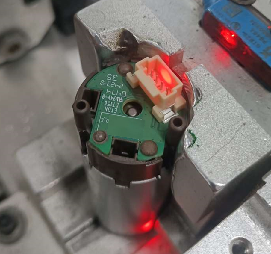
Welding circuit board plastic structural parts.
At the same time, with the help of a dedicated control system, precise heat control and local heating during the transmission welding process can be achieved, the welding quality is consistent, and adverse effects on surrounding materials are avoided. It is widely used in automotive parts, medical equipment, electronic components and other industries. Welding of precision plastic parts.
PC+ABS plastic welding test
In actual operation, in order to ensure weld quality and sufficient melting depth, it is necessary to comprehensively consider the relationship between welding speed and laser power to find the optimal process window.
Welding PC and ABS plastics were tested. The two plastic parts were first stacked on a carrier and clamped using a clamp to apply pressure.
When the laser output power is adjusted to 300W and the welding speed is set to 20mm/s (up to 10000mm/s), the two layers of plastic are welded successfully, the weld seam is evenly fused, the weld seam width is moderate, the sealing is good, and the tensile test strength reaches Require.
The laser output power remains unchanged at 300W. When the welding speed is reduced and adjusted to 10mm/s, the two layers of plastic are successfully welded, the welds are evenly fused, the welds are wide, and the sealing is good; however, due to the excessive temperature of the molten pool, it may cause Part of the material decomposes, resulting in reduced weld strength.
When the power is adjusted to 200W and the welding speed is set to 20mm/s, the weld width is moderate, the fusion is good, the sealing is good, and the tensile test strength is lower than the welding strength at high power.
Laser welding advantages
The processes of laser welding and fusion bonding are similar, but the advantages of the former are more obvious:
First of all, it has high precision. The laser spot is small and highly uniform. It can accurately align smaller welding parts, quickly convert laser energy into the energy required for welding, achieve precision welding, and greatly improve welding efficiency. . Combined with the professionally designed welding head, it can ensure that the laser energy is fully absorbed in the welding area and ensure the strength of the welding joint.
Secondly, the heat-affected zone is small, which can avoid thermal damage to the plastic surface during the welding process and maintain the transparency and smoothness of the material. This allows the product after light-transmitting welding to maintain its original appearance characteristics and enhance the structural stability.
Third, it solves the contradiction between welding speed and welding quality in traditional welding methods, can complete large-area welding in a short time, and greatly improves production efficiency. A welding job that originally took several hours can now be easily completed in just a few or dozens of minutes, saving a lot of time and cost.
In addition, the non-contact welding operation avoids the mechanical stress and vibration caused by traditional connection methods, protects the integrity of the plastic surface, and ensures the precision of the weld. The connection between materials is tighter and more reliable, and the sealing is excellent. , meeting high-standard product requirements such as waterproofing and dustproofing.
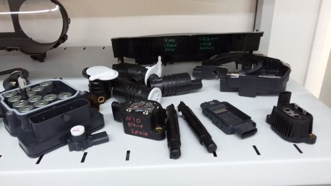
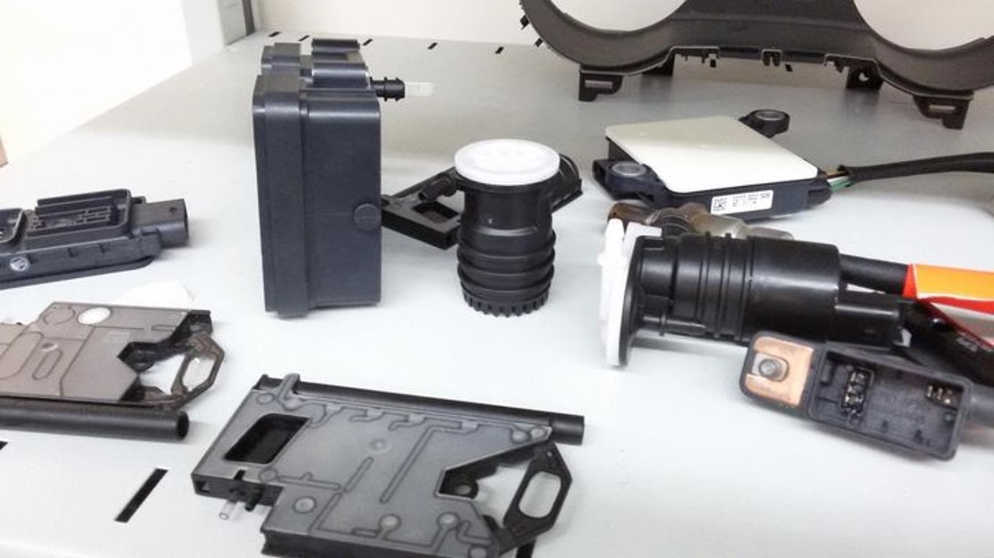
Figure 4: Welding automotive plastic parts
summary
At present, the 980nm semiconductor laser has shown strong market potential and application value. It is a powerful tool for plastic welding, especially in automotive plastic welding, bringing efficient and stable welding results. In interior welding, it can be used for welding dashboards, center consoles, etc.; in exterior parts welding, it can easily weld door handles, lights, etc.; in welding automotive electronic parts, 980nm semiconductor lasers also perform well. , can be used for plastic welding of many electronic components, significantly improving the connection strength and sealing, ensuring the stability and reliability of each component. In the future, with the continuous development of functions, 980nm products will also usher in wider applications.